A Momentary Variation of Voltage From One Logic Level to the Opposite Level and Back Again
Transistor–transistor logic (TTL) is a logic family built from bipolar junction transistors. Its name signifies that transistors perform both the logic function (the first "transistor") and the amplifying office (the second "transistor"), as opposed to resistor–transistor logic (RTL) or diode–transistor logic (DTL).
TTL integrated circuits (ICs) were widely used in applications such as computers, industrial controls, examination equipment and instrumentation, consumer electronics, and synthesizers. Sometimes TTL-compatible logic levels are non associated straight with TTL integrated circuits, for example, they may be used at the inputs and outputs of electronic instruments.[1]
Subsequently their introduction in integrated circuit form in 1963 by Sylvania Electric Products, TTL integrated circuits were manufactured past several semiconductor companies. The 7400 series past Texas Instruments became particularly pop. TTL manufacturers offered a wide range of logic gates, flip-flops, counters, and other circuits. Variations of the original TTL circuit design offered higher speed or lower power dissipation to allow design optimization. TTL devices were originally made in ceramic and plastic dual in-line package(south) and in flat-pack form. Some TTL fries are now also made in surface-mountain technology packages.
TTL became the foundation of computers and other digital electronics. Even after Very-Large-Scale Integration (VLSI) CMOS integrated excursion microprocessors fabricated multiple-chip processors obsolete, TTL devices still found extensive use as mucilage logic interfacing between more than densely integrated components.
History [edit]
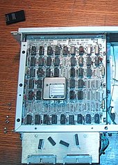
A real-time clock built of TTL chips effectually 1979
TTL was invented in 1961 by James Fifty. Buie of TRW, which declared information technology, "especially suited to the newly developing integrated circuit pattern technology." The original name for TTL was transistor-coupled transistor logic (TCTL).[two] The first commercial integrated-excursion TTL devices were manufactured past Sylvania in 1963, chosen the Sylvania Universal High-Level Logic family (SUHL).[three] The Sylvania parts were used in the controls of the Phoenix missile.[3] TTL became popular with electronic systems designers afterward Texas Instruments introduced the 5400 series of ICs, with military temperature range, in 1964 and the later 7400 serial, specified over a narrower range and with inexpensive plastic packages, in 1966.[4]
The Texas Instruments 7400 family became an industry standard. Compatible parts were made past Motorola, AMD, Fairchild, Intel, Intersil, Signetics, Mullard, Siemens, SGS-Thomson, Rifa, National Semiconductor,[5] [6] and many other companies, even in the Eastern Bloc (Soviet Union, German democratic republic, Poland, Czechoslovakia, Hungary, Romania - for details see 7400 series). Non simply did others make compatible TTL parts, but compatible parts were fabricated using many other excursion technologies as well. At least one manufacturer, IBM, produced non-uniform TTL circuits for its own use; IBM used the engineering science in the IBM System/38, IBM 4300, and IBM 3081.[7]
The term "TTL" is practical to many successive generations of bipolar logic, with gradual improvements in speed and power consumption over virtually two decades. The most recently introduced family 74Fxx is still sold today (as of 2019), and was widely used into the tardily 90s. 74AS/ALS Advanced Schottky was introduced in 1985.[8] As of 2008, Texas Instruments continues to supply the more general-purpose chips in numerous obsolete technology families, albeit at increased prices. Typically, TTL chips integrate no more than than a few hundred transistors each. Functions within a single parcel mostly range from a few logic gates to a microprocessor fleck-slice. TTL too became important because its low cost made digital techniques economically practical for tasks previously done by analog methods.[nine]
The Kenbak-i, ancestor of the first personal computers, used TTL for its CPU instead of a microprocessor scrap, which was not available in 1971.[10] The Datapoint 2200 from 1970 used TTL components for its CPU and was the footing for the 8008 and later the x86 education ready.[eleven] The 1973 Xerox Alto and 1981 Star workstations, which introduced the graphical user interface, used TTL circuits integrated at the level of arithmetic logic units (ALUs) and bitslices, respectively. Near computers used TTL-compatible "glue logic" between larger fries well into the 1990s. Until the advent of programmable logic, detached bipolar logic was used to epitome and emulate microarchitectures under evolution.
Implementation [edit]
Cardinal TTL gate [edit]

Two-input TTL NAND gate with a uncomplicated output stage (simplified)
TTL inputs are the emitters of bipolar transistors. In the case of NAND inputs, the inputs are the emitters of multiple-emitter transistors, functionally equivalent to multiple transistors where the bases and collectors are tied together.[12] The output is buffered by a common emitter amplifier.
Inputs both logical ones. When all the inputs are held at high voltage, the base–emitter junctions of the multiple-emitter transistor are contrary-biased. Unlike DTL, a modest "collector" current (approximately 10µA) is fatigued by each of the inputs. This is because the transistor is in reverse-active mode. An approximately constant current flows from the positive track, through the resistor and into the base of operations of the multiple emitter transistor.[xiii] This current passes through the base of operations–emitter junction of the output transistor, allowing information technology to conduct and pulling the output voltage low (logical zero).
An input logical null. Note that the base of operations–collector junction of the multiple-emitter transistor and the base–emitter junction of the output transistor are in series between the lesser of the resistor and ground. If ane input voltage becomes zip, the corresponding base of operations–emitter junction of the multiple-emitter transistor is in parallel with these ii junctions. A phenomenon chosen current steering means that when ii voltage-stable elements with different threshold voltages are connected in parallel, the current flows through the path with the smaller threshold voltage. That is, current flows out of this input and into the aught (depression) voltage source. As a issue, no current flows through the base of the output transistor, causing it to finish conducting and the output voltage becomes high (logical one). During the transition the input transistor is briefly in its agile region; and so information technology draws a large current away from the base of the output transistor and thus quickly discharges its base of operations. This is a critical reward of TTL over DTL that speeds up the transition over a diode input structure.[xiv]
The chief disadvantage of TTL with a simple output stage is the relatively high output resistance at output logical "1" that is completely determined by the output collector resistor. It limits the number of inputs that tin be continued (the fanout). Some advantage of the simple output stage is the high voltage level (up to FiveCC) of the output logical "1" when the output is not loaded.
A mutual variation omits the collector resistor of the output transistor, making an open-collector output. This allows the designer to fabricate logic past connecting the open-collector outputs of several logic gates together and providing a single external pull-up resistor. If any of the logic gates becomes logic low (transistor conducting), the combined output will be low. Examples of this type of gate are the 7401[15] and 7403 series. Open-collector outputs of some gates have a college maximum voltage, such as 15 V for the 7426,[16] useful when driving other than TTL loads.
TTL with a "totem-pole" output phase [edit]

Standard TTL NAND with a "totem-pole" output stage, one of four in 7400
To solve the trouble with the loftier output resistance of the simple output stage the second schematic adds to this a "totem-pole" ("push–pull") output. It consists of the two n-p-due north transistors Five3 and Fiveiv, the "lifting" diode V5 and the current-limiting resistor R3 (run into the figure on the right). It is driven by applying the same current steering idea as above.
When V2 is "off", V4 is "off" as well and V3 operates in active region every bit a voltage follower producing high output voltage (logical "ane").
When Vtwo is "on", it activates Fiveiv, driving low voltage (logical "0") to the output. Again there is a current-steering effect: the series combination of V2'due south C-East junction and V4's B-E junction is in parallel with the serial of Vthree B-E, 5v's anode-cathode junction, and V4 C-E. The 2d serial combination has the college threshold voltage, so no electric current flows through it, i.eastward. V3 base of operations current is deprived. Transistor V3 turns "off" and it does not touch on the output.
In the middle of the transition, the resistor Riii limits the current flowing directly through the series continued transistor 5iii, diode Vfive and transistor V4 that are all conducting. It also limits the output electric current in the instance of output logical "1" and short connectedness to the ground. The strength of the gate may be increased without proportionally affecting the ability consumption by removing the pull-up and pull-down resistors from the output stage.[17] [eighteen]
The main advantage of TTL with a "totem-pole" output stage is the low output resistance at output logical "1". It is determined past the upper output transistor Fiveiii operating in active region as an emitter follower. The resistor R3 does not increment the output resistance since it is connected in the Fivethree collector and its influence is compensated by the negative feedback. A disadvantage of the "totem-pole" output phase is the decreased voltage level (no more than than 3.5 V) of the output logical "ane" (fifty-fifty if the output is unloaded). The reason of this reduction are the voltage drops beyond the 53 base–emitter and Five5 anode–cathode junctions.
Interfacing considerations [edit]
Like DTL, TTL is a current-sinking logic since a current must exist drawn from inputs to bring them to a logic 0 voltage level. The driving phase must blot up to ane.half-dozen mA from a standard TTL input while not allowing the voltage to rise to more than than 0.iv volts.[19] The output stage of the most mutual TTL gates is specified to function correctly when driving up to ten standard input stages (a fanout of 10). TTL inputs are sometimes just left floating to provide a logical "ane", though this usage is not recommended.[20]
Standard TTL circuits operate with a 5-volt ability supply. A TTL input signal is divers every bit "low" when betwixt 0 5 and 0.8 V with respect to the ground final, and "loftier" when between 2 V and 5CC (5 Five),[21] [22] and if a voltage signal ranging between 0.8 V and 2.0 5 is sent into the input of a TTL gate, there is no certain response from the gate and therefore it is considered "uncertain" (precise logic levels vary slightly between sub-types and past temperature). TTL outputs are typically restricted to narrower limits of between 0.0 V and 0.4 V for a "low" and between 2.4 V and VCC for a "high", providing at to the lowest degree 0.4 V of racket immunity. Standardization of the TTL levels is so ubiquitous that complex circuit boards often contain TTL chips made past many different manufacturers selected for availability and cost, compatibility being assured. Two excursion board units off the aforementioned assembly line on different successive days or weeks might have a unlike mix of brands of chips in the same positions on the lath; repair is possible with chips manufactured years later than original components. Within usefully broad limits, logic gates can be treated as ideal Boolean devices without concern for electrical limitations. The 0.4V noise margins are adequate because of the low output impedance of the commuter stage, that is, a large corporeality of noise power superimposed on the output is needed to drive an input into an undefined region.
In some cases (eastward.g., when the output of a TTL logic gate needs to be used for driving the input of a CMOS gate), the voltage level of the "totem-pole" output phase at output logical "1" can be increased closer to VCC by connecting an external resistor between the V4 collector and the positive rails. It pulls upward the Vv cathode and cuts-off the diode.[23] However, this technique actually converts the sophisticated "totem-pole" output into a uncomplicated output stage having pregnant output resistance when driving a high level (adamant by the external resistor).
Packaging [edit]
Similar near integrated circuits of the menses 1963–1990, commercial TTL devices are usually packaged in dual in-line packages (DIPs), unremarkably with xiv to 24 pins,[24] for through-pigsty or socket mounting. Epoxy plastic (PDIP) packages were frequently used for commercial temperature range components, while ceramic packages (CDIP) were used for military temperature range parts.
Beam-lead chip dies without packages were made for assembly into larger arrays as hybrid integrated circuits. Parts for armed services and aerospace applications were packaged in flatpacks, a form of surface-mountain parcel, with leads suitable for welding or soldering to printed circuit boards. Today[ when? ], many TTL-uniform devices are bachelor in surface-mount packages, which are available in a wider array of types than through-hole packages.
TTL is particularly well suited to bipolar integrated circuits because boosted inputs to a gate simply required additional emitters on a shared base region of the input transistor. If individually packaged transistors were used, the cost of all the transistors would discourage one from using such an input construction. But in an integrated circuit, the additional emitters for extra gate inputs add together only a small surface area.
At least one estimator manufacturer, IBM, built its own flip chip integrated circuits with TTL; these fries were mounted on ceramic multi-bit modules.[25] [26]
Comparison with other logic families [edit]
TTL devices consume substantially more than ability than equivalent CMOS devices at rest, but power consumption does not increase with clock speed equally rapidly every bit for CMOS devices.[27] Compared to gimmicky ECL circuits, TTL uses less power and has easier design rules simply is substantially slower. Designers can combine ECL and TTL devices in the same organisation to achieve all-time overall performance and economic system, but level-shifting devices are required betwixt the ii logic families. TTL is less sensitive to harm from electrostatic discharge than early CMOS devices.
Due to the output construction of TTL devices, the output impedance is asymmetrical between the high and low state, making them unsuitable for driving manual lines. This drawback is commonly overcome by buffering the outputs with special line-commuter devices where signals need to be sent through cables. ECL, by virtue of its symmetric depression-impedance output structure, does not have this drawback.
The TTL "totem-pole" output structure oftentimes has a momentary overlap when both the upper and lower transistors are conducting, resulting in a substantial pulse of current drawn from the power supply. These pulses can couple in unexpected ways between multiple integrated excursion packages, resulting in reduced racket margin and lower functioning. TTL systems usually accept a decoupling capacitor for every one or ii IC packages, so that a current pulse from ane TTL fleck does not momentarily reduce the supply voltage to another.
Since the mid 1980s, several manufacturers supply CMOS logic equivalents with TTL-compatible input and output levels, ordinarily begetting office numbers similar to the equivalent TTL component and with the same pinouts. For case, the 74HCT00 serial provides many driblet-in replacements for bipolar 7400 series parts, but uses CMOS technology.
Sub-types [edit]
Successive generations of technology produced compatible parts with improved power consumption or switching speed, or both. Although vendors uniformly marketed these various product lines equally TTL with Schottky diodes, some of the underlying circuits, such equally used in the LS family, could rather be considered DTL.[28]
Variations of and successors to the basic TTL family, which has a typical gate propagation delay of 10ns and a power dissipation of 10 mW per gate, for a power–filibuster product (PDP) or switching energy of about 100 pJ, include:
- Low-power TTL (Fifty), which traded switching speed (33ns) for a reduction in power consumption (1 mW) (at present essentially replaced by CMOS logic)
- High-speed TTL (H), with faster switching than standard TTL (6ns) but significantly higher power dissipation (22 mW)
- Schottky TTL (S), introduced in 1969, which used Schottky diode clamps at gate inputs to prevent charge storage and improve switching time. These gates operated more quickly (3ns) but had higher ability dissipation (19 mW)
- Depression-power Schottky TTL (LS) – used the higher resistance values of low-power TTL and the Schottky diodes to provide a good combination of speed (9.5ns) and reduced power consumption (2 mW), and PDP of about 20 pJ. Probably the well-nigh common type of TTL, these were used equally glue logic in microcomputers, essentially replacing the sometime H, Fifty, and S sub-families.
- Fast (F) and Advanced-Schottky (AS) variants of LS from Fairchild and TI, respectively, circa 1985, with "Miller-killer" circuits to speed upwardly the low-to-high transition. These families achieved PDPs of 10 pJ and four pJ, respectively, the lowest of all the TTL families.
- Depression-voltage TTL (LVTTL) for 3.3-volt ability supplies and memory interfacing.
Nigh manufacturers offer commercial and extended temperature ranges: for example Texas Instruments 7400 series parts are rated from 0 to 70 °C, and 5400 series devices over the military-specification temperature range of −55 to +125 °C.
Special quality levels and high-reliability parts are available for military and aerospace applications.
Radiation-hardened devices (for instance from the SNJ54 series) are offered for space applications.
Applications [edit]
Before the appearance of VLSI devices, TTL integrated circuits were a standard method of structure for the processors of minicomputer and mainframe computers; such every bit the December VAX and Data Full general Eclipse, and for equipment such equally motorcar tool numerical controls, printers and video brandish terminals. Every bit microprocessors became more functional, TTL devices became important for "glue logic" applications, such as fast jitney drivers on a motherboard, which tie together the part blocks realized in VLSI elements.
Analog applications [edit]
While originally designed to handle logic-level digital signals, a TTL inverter can be biased as an analog amplifier. Connecting a resistor between the output and the input biases the TTL element equally a negative feedback amplifier. Such amplifiers may exist useful to catechumen analog signals to the digital domain only would not ordinarily exist used where analog amplification is the chief purpose.[29] TTL inverters can also be used in crystal oscillators where their analog amplification ability is significant.
A TTL gate may operate inadvertently equally an analog amplifier if the input is connected to a slowly changing input signal that traverses the unspecified region from 0.viii V to two V. The output can be erratic when the input is in this range. A slowly changing input like this can also cause excess power dissipation in the output circuit. If such an analog input must be used, there are specialized TTL parts with Schmitt trigger inputs available that will reliably convert the analog input to a digital value, finer operating every bit a one fleck A to D converter.
See also [edit]
- List of 7400 serial integrated circuits
References [edit]
- ^ Eren, H. (2003), Electronic Portable Instruments: Design and Applications, CRC Press, ISBN0-8493-1998-6
- ^ US 3283170, Buie, James L., "Coupling transistor logic and other circuits", issued 1966-xi-01, assigned to TRW Semiconductors, Inc.
- ^ a b The Reckoner History Museum. 1963 - Standard Logic Families Introduced. 2007. Retrieved 16 April 2008.
- ^ Lojek, Bo (2006), History of semiconductor engineering, Springer, pp. 212–215, ISBNiii-540-34257-five
- ^ Applied science Staff. The TTL Data Book for Design Engineers. 1st Ed. Dallas: Texas Instruments. 1973.
- ^ Turner, Fifty. West., ed. (1976), Electronics Engineer'southward Reference Volume (quaternary ed.), London: Newnes-Butterworth, ISBN0408001682
- ^ , p. five.
- ^ Texas Instruments. Advanced Schottky Family. 1985. Retrieved 17 September 2008.
- ^ Lancaster, D (1975), TTL Cookbook, Indianapolis: Howard W. Sams and Co., p. preface, ISBN0-672-21035-5
- ^ Klein, E. Kenbak-1. Vintage-Computer.com. 2008.
- ^ Lamont Woods, "Forgotten PC history: The truthful origins of the personal estimator" Archived 2008-08-14 at the Wayback Machine, Computerworld, 8 August 2008
- ^ Gray, Paul E.; Searle, Campbell Fifty. (1969), Electronic Principles Physics, Models, and Circuits (1st ed.), Wiley, p. 870, ISBN978-0471323983
- ^ Buie 1966, column 4
- ^ Millman, J. (1979), Microelectronics Digital and Analog Circuits and Systems, New York: McGraw-Loma Book Company, p. 147, ISBN0-07-042327-X
- ^ SN7401 datasheet – Texas Instruments
- ^ SN7426 datasheet – Texas Instruments
- ^ Transistor–Transistor Logic (TTL). siliconfareast.com. 2005. Retrieved 17 September 2008. p. 1.
- ^ Tala, D. K. Digital Logic Gates Part-V. asic-world.com. 2006.
- ^ SN7400 datasheet - Texas Instruments
- ^ Haseloff, Eilhard. "Designing With Logic" (PDF). TI.com. Texas Instruments Incorporated. pp. half-dozen–vii. Retrieved 27 October 2018.
- ^ TTL logic levels
- ^ "DM7490A Decade and Binary Counter" (PDF). Fairchild. Retrieved 14 October 2016.
- ^ TTL-to-CMOS Interfacing Techniques Archived 2010-09-19 at the Wayback Machine
- ^ Marston, R. Thou. (2013). Modern TTL Circuits Transmission. Elsevier. p. 16. ISBN9781483105185.
[74-serial] devices are commonly encapsulated in a plastic 14-pin, 16-pin, or 24-pin dual-in-line packet (DIP)
- ^ Rymaszewski, Due east. J.; Walsh, J. L.; Leehan, Thou. Due west. (1981), "Semiconductor Logic Technology in IBM", IBM Journal of Research and Development, 25 (5): 603–616, doi:10.1147/rd.255.0603
- ^ Seraphim, D. P.; Feinberg, I. (1981), "Electronic Packaging Evolution in IBM", IBM Journal of Inquiry and Evolution, 25 (5): 617–630, doi:10.1147/rd.255.0617
- ^ Horowitz, Paul; Hill, Winfield (1989), The Fine art of Electronics (2d ed.), Cambridge University Printing, p. 970, ISBN0-521-37095-7 states, "...CMOS devices consume power proportional to their switching frequency...At their maximum operating frequency they may use more ability than equivalent bipolar TTL devices."
- ^ Ayers, J. UConn EE 215 notes for lecture 4. Harvard University faculty web page. Annal of web page from University of Connecticut. n.d. Retrieved 17 September 2008.
- ^ Wobschall, D. (1987), Circuit Blueprint for Electronic Instrumentation: Analog and Digital Devices from Sensor to Display (2d ed.), New York: McGraw Hill, pp. 209–211, ISBN0-07-071232-8
Further reading [edit]
- Lessons in Electrical Circuits - Book IV - Digital; Tony Kuphaldt; Open Book Projection; 508 pages; 2007. (Chapter three Logic Gates)
External links [edit]
| | Wikimedia Eatables has media related to TTL. |
- Fairchild Semiconductor. An Introduction to and Comparison of 74HCT TTL Uniform CMOS Logic (Awarding Notation 368). 1984. (for relative ESD sensitivity of TTL and CMOS.)
- Texas Instruments logic family unit awarding notes
mcdonnellfromight.blogspot.com
Source: https://en.wikipedia.org/wiki/Transistor%E2%80%93transistor_logic
0 Response to "A Momentary Variation of Voltage From One Logic Level to the Opposite Level and Back Again"
Post a Comment